With over 30 years of experience and thousands of analyses conducted, SERMA Technologies has developed a unique expertise that allows us to work on all types of electronic components, boards, and systems.
Our expertise spans a wide range of technologies and sectors, from aerospace to automotive, as well as energy and defense.
With our laboratories equipped with state-of-the-art technologies and our recognized expertise, we support our clients in their most complex technical challenges, while ensuring reliable and precise results.
We offer advanced expertise services to guarantee the quality, reliability, and compliance of your products, regardless of their complexity level:
DPA & construction analysis
DPA (Destructive Physical Analysis)
Our DPA service allows us to evaluate the quality of your products by comparing them to stringent standards such as those established by MIL (Military Standards) or ESA/ESCC (European Space Agency / European Space Components Coordination).
This in-depth analysis provides valuable insights into the compliance and reliability of your electronic components, ensuring their performance in critical environments.
Construction Analysis
We also conduct construction analysis to assess the quality of your products against the state of the art. This method identifies the strengths and weaknesses of design and manufacturing, ensuring that your products meet the highest industry standards.
Our analyses combine both non-destructive testing (NDT) and destructive testing (DT) methods to offer a comprehensive evaluation. They are essential to ensure the reliability and durability of your products in critical applications.
Our non-destructive testing methods
- Visual Inspection: detection of surface and assembly defects,
- Radiography: examination of internal structures to identify voids and solder defects,
- Acoustic Microscopy: analysis of internal defects using ultrasonic waves.
Our destructive testing methods
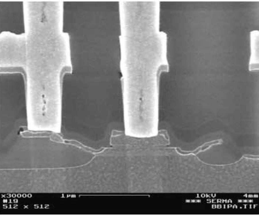
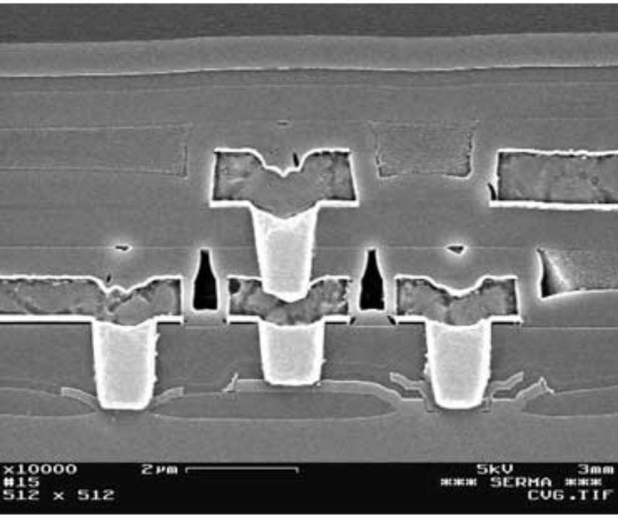
- Microsectioning: detailed examination of the internal layers of a component,
- Shear Testing: evaluation of joint strength,
- Tensile Testing: measurement of break resistance,
- Solderability Testing: verification of solder quality.
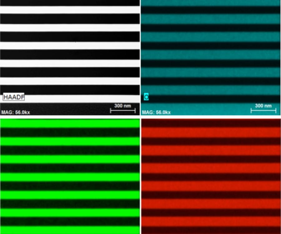
Material characterisation
Material characterization is a crucial step in the development and optimization of electronic components.
At SERMA Technologies, we provide our expertise and state-of-the-art equipment to thoroughly analyze the physical, chemical, electrical, and mechanical properties of the materials used in electronic devices.
Our specialized laboratory allows for the evaluation of various materials, including metals, polymers, ceramics, and semiconductors.
With advanced equipment, we conduct:
- Chemical Analysis: identification of elements and impurities.
- Structural Studies: observation of microstructures and defects.
- Mechanical and Thermal Characterization: measurement of hardness, strength, conductivity, and thermal stability.
- Electrical Characterization: assessment of electrical properties to ensure performance and reliability.
Material characterization ensures that the materials used meet the expected standards of quality, reliability, and performance. It is also essential for understanding how materials behave under different environmental conditions and for anticipating their degradation over time.
At SERMA, we support our clients across various sectors, such as aerospace, automotive, and energy, in selecting the most suitable materials for their applications and optimizing the performance of their electronic systems.
Failure analysis
Failure analysis enables the understanding of failure modes and mechanisms of electronic components.
At SERMA Technologies, we offer in-depth electrical and physical analyses to diagnose the underlying causes of failures.
This approach not only resolves existing issues but also anticipates and prevents potential future failures.
We have a wide range of techniques and tools for sample preparation, observation, and analysis.
Our techniques and tools for failure analysis
- Electrical Testing
- Optical Microscopy
- Acoustic Microscopy
- 2D and 3D X-Ray
- Radiography – X-Ray Laminography
- Infrared Thermography
- Opening of Enclosures (Mechanical, Chemical, etc.)
- Microsectioning
- Slice and View
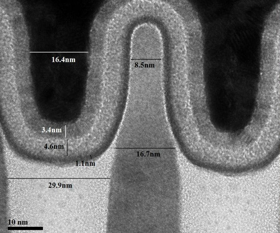
- SEM (Scanning Electron Microscopy) Observations
- Material Analysis by EDX
- TEM (Transmission Electron Microscopy) Observations
- Defect localisation
These tools and techniques allow us to provide comprehensive and precise analyses, ensuring the reliability and durability of your electronic products. Our expertise in failure analysis positions us as a key partner in optimizing the performance and quality of your systems.
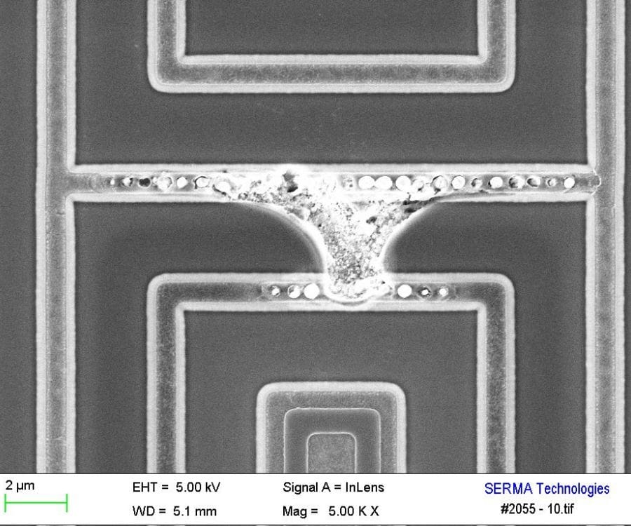
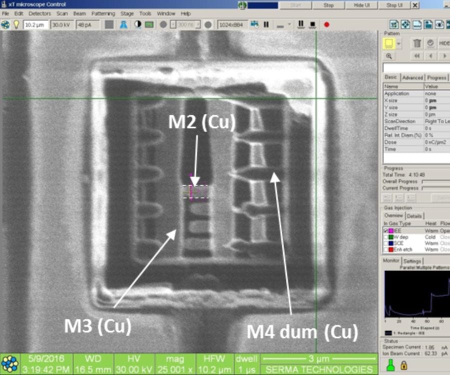
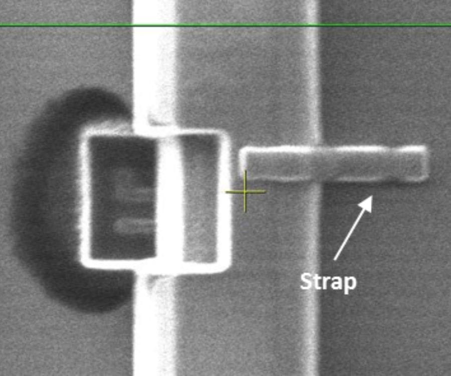
Circuit edit
Thanks to FIB (Focused Ion Beam) technology, we have access to the internal functions of a circuit. This technique allows us to cut metal lines and add connections or metal probe pads.
In the context of design modifications, debugging, or evaluating electrical performance, circuit modification with FIB provides the opportunity to test specific adjustments without the need to refabricate the chip or produce numerous lithographic masks.
Main chemistry
- Selective etching of aluminium and other metals
- Selective copper etching
- Selective dielectric etching
- Metal deposition
- Dielectric deposition
Key points of circuit modification:
- Matrix alignment (GDS II) for precise modifications
- Direct circuit modification: cuts and straps, for mature Al technologies or for more advanced Cu / lowk technologies. Metal filling is a challenge, but it can be managed.
- Metal probe padding for measurements of two or more point probes
- An open laboratory with your presence is a possibility for personalized needs and specific requests.
- Location of a fault by potential contrast
- Modifications on the reverse side are possible
Additional information:
- We work with several types of devices: chip, case, wafer, PCB
- Possibility of decapping the preliminary package
- We can test the modifications internally with our probe system.
- Delivery time reduced to 3 days
- Standard delivery time: 2 weeks
- SERMA repository, FTP client or encryption solutions (OpenPGP, S/MIME) to secure the communication of your GDS II file